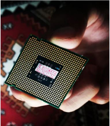
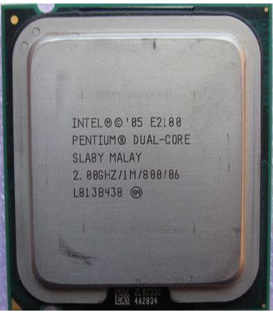
Intel Pentium Dual Core
The microprocessor is a multipurpose, programmable, and clock-driven integrated circuit. This IC can read binary instructions from any storage device called memory. It also accepts binary data as input, processes data according to instructions, and provides results as output.
Among several microprocessors invented till date let us talk about “Intel Pentium Dual Core E2180” processor. Intel is the top processor brand making microprocessors from its date of invention.The name string on CPU of this processor is Intel(R) Pentium(R) Dual CPU E2180 @ 2.00GHz.The name Pentium is originally derived from the Greek word pente , meaning “five”, a reference to the prior numeric naming convention of Intel’s 80×86 architecture processors (8086–80486) from 2006 to 2009, with the Latin ending -ium since the processor would otherwise have been named 80586 using that convention.
Dual Core represents the number of independent central processing units in a single computing component.
E2180 is the specific processor number. Intel processor numbers are not a measure of performance. They differentiate features within each processor family, not across different processor families. Over time processor numbers will increment based on changes in clock, speed, cache, FSB, or other features.
The model numbers can be used to identify only basic features as mentioned and most important characteristics, and may not be used to identify all features/parameters of the CPU.
History And Release
It was launched after Pentium M and Pentium D microprocessors. In 2006, Intel announced a plan to return the Pentium trademark from retirement to the market, as a moniker of low-cost Core microarchitecture processors based on the single-core Conroe-L but with 1 MiB of cache.
The identification numbers for those planned Pentiums were similar to the numbers of the latter Pentium Dual-Core microprocessors, but with the first digit “1”, instead of “2”, suggesting their single-core functionality.
A single-core Conroe-L with 1 MiB cache was deemed as not strong enough to distinguish the planned Pentiums from the Celerons, so it was replaced by dual-core CPUs, adding “Dual-Core” to the line’s name.
On June 3, 2007, Intel released the desktop Pentium Dual-Core branded processors known as the Pentium E2140 and E2160. An E2180 model was released later in September 2007. It had $84 price when it was released. It falls under Allendale dual (65nm) intel pentium dual core family released on Jun 2007 .
Pentium (2009) was its succesor and intel has released so many microprocessors after it discontiuned.
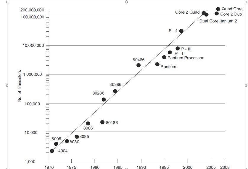
Evolution of Microprocessor based on number of transistors till 2008 can be shown below:
Multi core over single core:
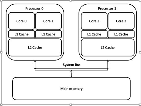
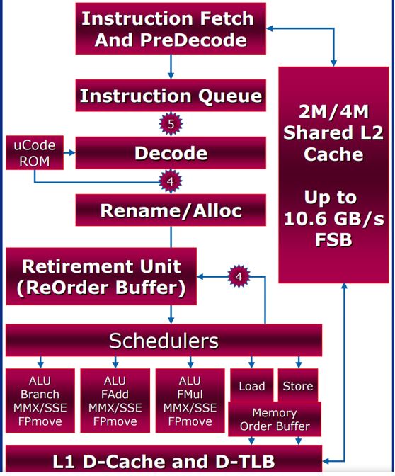
Architectures such as the current Intel pentium dual core, as shown in Figure 1, provide a shared cache between the different cores on the same die. This makes communication even simpler by eliminating the need for complicated cache-coherency protocols.
In a shared memory multiprocessor system with a separate cache memory for each processor, it is possible to have many copies of shared data: one copy in the main memory and one in the local cache of each processor that requested it. When one of the copies of data is changed, the other copies must reflect that change.
Cache coherence is the discipline which ensures that the changes in the values of shared operands (data) are propagated throughout the system in a timely fashion.
Microarchitecture:
The intel pentium dual core processors were based on intel core microarchitecture. The Intel Core microarchitecture (previously known as the Next-Generation Micro-Architecture, or NGMA) is a multi-core processor microarchitecture unveiled by Intel in 2006.
The E2180 uses the 64-bit Allendale core in desktop, which includes 2 MB of native L2 cache, with half disabled leaving only 1 MB. This compares to the higher end Conroe core which features 4 MB L2 Cache natively. Intel has shifted its product lines having the Core 2 line as Mainstream/Performance, Pentium Dual-Core as Mainstream, and the new Celeron (based on the Conroe-L core) as Budget/Value.
These CPUs are highly overclockable. The Penryn pipeline is 12–14 stages long, a signature feature of wide order execution cores. Penryn’s successor, Nehalem has 20-24 pipeline stages.
Core’s execution unit is 4 issues wide, compared to the 3-issue cores of P6, Pentium M, and 2-issue cores of NetBurst microarchitectures. Where dual core design is a new architecture with linked L1 cache and shared L2 cache engineered for maximum performance per watt and improved scalability.
- Manufacturing process is of 0.065 micron.
- Floating Point Unit is Integrated in this microprocessor.
- Core Stepping: L2, M0 (Allendale)
Over course of its life, each microprocessor core could be refined or tweaked multiple times without changing or adding any major processor features. The purpose of the tweaks is to eliminate existing errata (errors in microprocessor logic), improve processor’s stability or reliability, and/or enhance some electrical, thermal or other processor characteristics. Each new core revision with these changes are referred to as a core stepping, and the changes never affect CPU performance.
- Cache: 1 MB L2 cache.
Level 1 cache, often abbreviated as L1 cache( also called primary cache), is a static memory integrated with processor core that is used to store information recently accessed by a processor. The purpose of L1 cache is to improve data access speed in cases when the CPU accesses the same data multiple times.
L1 Cache size:2 x 32 KB 8-way set associative instruction caches and 2 x 32 KB 8-way set associative data caches.
Whereas Level 2 cache, often abbreviated as L2 cache( also called secondary cache), is a memory that is used to store recently accessed information. The goal of having the L2 cache is to reduce data access time in cases when the same data was already accessed before. It is not as fast as the level 1 cache, although it is usually much larger. All data that is requested from level 2 cache is copied to level 1 cache.
L2 cache size: 1 MB 4-way set associative shared cache
Regarding security features Enhanced Virus Protection (EVP) / Execute Disable (XD) bit is inbuilt to prevent execution of malicious code in program data memory.
Pentium supports two modes
∗ Real mode
» Uses 16-bit addresses
» Runs 8086 programs
» Pentium acts as a faster 8086
∗ Protected mode
» 32-bit mode
» Native mode of Pentium
» Supports segmentation and paging
Specifications:
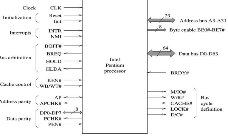
- Data I/O bus(D0 – D 63): All modern processors like pentium have a 64-bit i.e.8-byte wide data bus. Therefore, they can transfer 64 bits of data at a time to and from the motherboard chipset or system memory.
- Address Bus(A3 – A31): The address bus is the set of wires that carry the addressing information used to describe the memory location to which the data is being sent or from which the data is being retrieved. The pentium processor has 29 lines of address bus.
- It has 64bit wide integer and address processsing registers supporting 64-bit data types and addresses. Also low level data types like floating point numbers has same size.
More Specifications Of Intel Pentium Dual Core:
- Number of cores: 2 . Cores are the processing units each of which reads and executes program instructions.
- Number of threads: Each cpu core has 2 threads. They determine how many tasks your computer can perform at any given time.
- Processor Base Frequency: This processor has 2.00GHz frequency of CPU. The frequency specifies the operating (internal) frequency of CPU’s core. The higher the frequency is for a given CPU family, the faster the processor . It also represents CPU efficiency that is how many Instructions Per Clock (IPC) the CPU can process.
- FSB speed: Front side bus is often abbreviated as FSB is also called system BUS. It is an interface between microprocessor core and other computer components, such as memory, peripheral devices and other microprocessors. Microprocessor performance highly depends on the speed, width and latency of the system bus. It has quad rate data bus so the fsb speed of this processor is 800 Mhz.
- Clock Multiplier is 10 which is the Internal frequency of microprocessors is usually based on Front Side Bus frequency.
To calculate internal frequency the CPU multiplies bus frequency by certain number, which is called clock multiplier.
It’s important to note that for calculation the CPU uses actual bus frequency, and not effective bus frequency. To determine actual actual bus frequency this processor uses quad-data rate buses the effective bus speed should be divided by 4 for Intel.
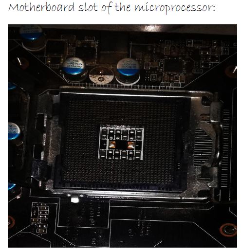
- Socket: It supports the LGA775 socket. LGA 775 (land grid array 775) is an Intel desktop CPU socket. It has 775 protruding pins which touch contact points on the underside of the processor (CPU).These are capable of doing Virtualization but only requires using VMware Workstation 12.
- TDP: The Thermal Design Power (TDP) is the average maximum power a processor can dissipate while running commercially available software. TDP is usually 20% – 30% lower than the CPU maximum power dissipation.It is 65W for this processor.
- VID: The voltage range if from 0.85 V to 1.5V.
- Minimum operating temperature: 5°C
- Maximum operating temperature of case: 73.3°C
- CPU part numbers supported:
HH80557PG0411M is an OEM/tray microprocessor.(English Version) and BX80557E2180 is a boxed processor with fan and heatsink ( Chinese version).
- Package Size: 37.5mm x 37.5mm
- Processing Die Size:77 mm^2
- Number of Processing Die Transistors: 105 million
Get user manual and documentation at https://www.intel.co.uk/content/www/uk/en/homepage.html